Solder Mask Application in Flexible Printed Circuit Board
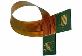
Flexible Printed Circuit Board
Printed circuit board (PCB) manufacturing is an incredibly complex process. It involves a number of different steps that must be done precisely and correctly in order to create an assembled board with high-quality components. One of the most critical processes is solder mask application. The solder mask is a layer of protective material that prevents the copper traces from making unintended connections, known as short circuits. This layer is applied to the surface of the PCB during the fabrication process, and it can be made in various colors and materials, depending on the manufacturer.
The most common type of solder mask is epoxy liquid, which is applied as a liquid before the flexible printed circuit board is soldered together and cured to dry. There are also dry film and curtain coating methods of application, which use vacuum lamination to reduce bubbles and adhere the mask to the board. Both types of solder mask have advantages and disadvantages, depending on the PCB design and manufacturer.
PCBs have many functions, and the primary function of solder mask is to protect the conductive traces from contact with other traces and the copper surface. Without this protection, the conductive traces would get damaged or shorted out during assembly and operation. Solder mask also helps to identify the traces on the board, which is essential for accurate component placement and alignment.
Solder Mask Application in Flexible Printed Circuit Board
Solder mask is typically green, which makes it easy for humans to see in daylight. The color was chosen because it is the least obtrusive to the copper surfaces of the board, but manufacturers use other colors as well. The best solder masks are compatible with a variety of surface finishes and assembly processes, including Hot Air Solder Leveling (HASL), Electroless Nickel Immersion Gold (ENIG), and Immersion Tin (ImSn).
There are several ways to apply the solder mask layer, with each method offering benefits and challenges. Traditionally, pattern printing was used to apply the solder mask to the printed circuit boards, but this technique is becoming less popular with the increasing number of fine-pitch components. Instead, most manufacturers now use a photoimageable solder mask (PISM) application process that exposes the bare copper to UV light except for those areas where components will be placed. The exposed areas are then “developed,” revealing openings for the component pads and holes. The dry mask is then removed, and the copper is etched.
The remaining copper is then plated with tin, which protects it from corrosion and provides additional electrical conductivity. Finally, the tin is coated with an insulating layer of epoxy resin. This epoxy is cured in the same way as the other insulating layers of the PCB, and the finished product is shipped to customers. As with all layered products, the final result depends on how well the PCB was constructed and manufactured, so it is important to test the finished product thoroughly. Testing can include a thermal shock test, which is a measure of the maximum temperature to which the board can be subjected.